
Our research group works at the interface of chemistry, physics, and engineering, with a focus on colloidal nanomaterials. We synthesize semiconductor nanocrystals from solution and integrate them directly into optoelectronic devices, creating a tight feedback loop between synthesis and device performance that accelerates materials development. Because our semiconductors are solution-processed, they act as functional inks that can be deposited on nearly any surface—enabling thin, lightweight, and low-cost optoelectronics beyond the limits of conventional technology. Target applications include next-generation perovskite solar cells, infrared photodetectors, and miniaturized optical spectrometers, where tailored nanomaterials directly improve both manufacturability and performance.
Materials Synthesis

We develop solution-based synthesis routes for semiconductor nanocrystals—including quantum dots such as PbS, HgTe, SnTe, and perovskites — as well as charge transport layers, processed either from colloidal nanocrystal dispersions (e.g., SnO₂) or from molecular solutions of organic semiconductors (e.g., Spiro-MeOTAD). Our focus lies on scalability, device stability, and precise control over composition & surface chemistry, combined with green and sustainable reaction design. The resulting inks enable low-cost, large-area fabrication of semiconductor thin films.
References
- M. J. Grotevent et al., Advanced Energy Materials 2024. https://doi.org/10.1002/aenm.202400456
- M. J. Grotevent et al., Chemistry of Materials 2025. https://doi.org/10.1021/acs.chemmater.5c01081
- M. J. Grotevent et al., Nature Photonics 2023. https://doi.org/10.1038/s41566-022-01088-7
- M. J. Grotevent et. al., Advanced Optical Materials 2019. https://doi.org/10.1002/adom.201900019
Perovskite Solar Cells
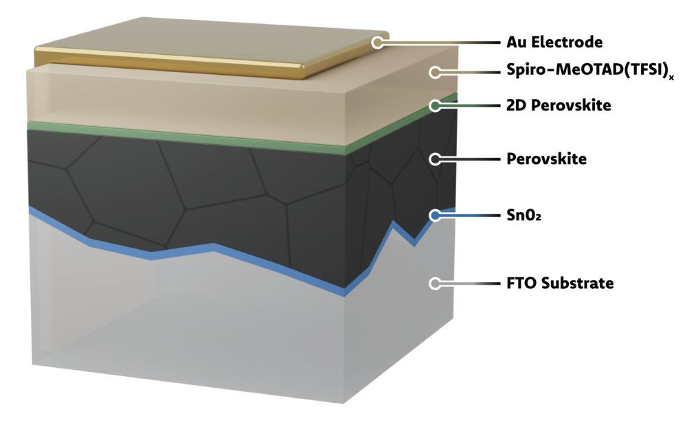
Perovskite photovoltaics are nearly on par with silicon in power conversion efficiency, but their industrial breakthrough demands materials and processes that scale to hundreds of square kilometers of modules per year—whether in tandem architectures, or single-junction (flexible) devices. We integrate nanocrystal-based charge transport layers and engineer the interfaces of n-i-p devices, where high thermal stability remains a particular challenge. Building on new insights into the thermal stability of individual layers (T₉₅ > 1,400 h at 85 °C), we aim to achieve high power conversion efficiency and high thermal stability simultaneously, using scalable deposition methods such as slot-die coating.
References
- M. J. Grotevent et al., Advanced Energy Materials 2024. https://doi.org/10.1002/aenm.202400456
- M. J. Grotevent et al., Chemistry of Materials 2025. https://doi.org/10.1021/acs.chemmater.5c01081
Miniaturized Optical Spectrometers

Quantum dot infrared photodetectors are ideal candidates for extreme miniaturization: when the detector is scaled down, the number of quantum dots decreases, but their intrinsic surface-to-volume ratio is expected to remain unchanged. We design such subwavelength-sized detectors and integrate them onto optical waveguides to realize chip-scale spectrometers. Our vision is a powerful miniaturized spectrometer in every smartphone, enabling everyday material analysis—from detecting harmful substances and fraudulent products to improving medical diagnostics.
References
M. J. Grotevent et al., Nature Photonics 2023. https://doi.org/10.1038/s41566-022-01088-7